
I have been building an Elecraft K2 kit radio, and I completed construction this Easter weekend.
When I ordered the kit, I didn’t order the internal ATU or the 100W amplifier option, as I already have an Elecraft KXPA100 amplifier with KXAT100 ATU. However, this amplifier is designed to work with the KX3 radio, and so to get it to work with the K2, I would need to build up a keying circuit.
Fortunately, Elecraft published on their website a neat solution for this. It consist of a couple of transistors mounted on some perfboard, which slots into a PCB header socket intended for the K2’s transporter interface module. Because I don’t have this option, my radio didn’t have the required header socket, but luckily the local electronics store sells suitable headers as part of their Arduino range. I picked up one of these headers, together with the other requisite parts.
The article on the Elecraft website provides a schematic, and some photos of the finished board, but they didn’t provide detailed information about how to build the circuit onto the perfboard. Fortunately, the circuit is quite simple, and wasn’t too hard to work out, but I decided to draw up a diagram which provides a better view of how the components are laid out and the physical connections are made.

The dotted lines show connections running under the board (except the gate lead of the 2N7000 JFET — that runs under the transistor, but along the top of the board).
I built the circuit in the following sequence:
1. put the 8 pin male header under the board on the left side, and solder one leg of the 2.2k resistor to the pin sticking out the top of the board at position A8. This then holds the header in place. The other leg on the 2.2k resistor goes through hole B5.
2. Sit the 10k resistor sitting up on end in hole C5, bend over the top leg and stick it through hole D4. Bend the legs underneath the board to hold the resistor in place.
3. Put a piece of hookup wire (eg. a component lead off-cut from when you built your K2) through hole D3. On the top of the board, bend the wire so it reaches the header pin 2 sticking through hole A2 and solder it to that pin.
4. Mount the right-angle molex receptor on top of the board through holes E1 and F1. Under the board, bend the hookup wire you installed in the previous step so it reaches the receptor pin sticking through hole F1, and solder to the receptor pin and trim. This will hold the receptor in place.
3. The Gate and Source legs of the 2N7000 JFET are the left two legs, if you hold the transistor with the flat face towards you. Bend those two legs backwards, and put the remaining leg (the Drain) in hole C1. Bend the Drain leg under the board down towards the resistors to hold the transistor in place.
4. Solder the Source leg (the left one you bent back) to the header pin 2, which sticks out of hole A2, and trim. Careful not to dislodge the hookup wire that is also soldered to that pin. Trim both the transistor lead and the hookup wire.
5. Solder the Gate leg (the middle one you bent back) to the header pin 1, which sticks out of hole A1, and trim.
6. The drain of the JFET which goes down through hole C1, and the resistor legs sticking through holes B5 and C5 should be bent so they all meet up. Solder the three leads together and trim.
7. The Emitter leg of the 2N2222 BJT is the left-most leg, if you hold the transistor with the flat face towards you. Bend that leg backwards, and put the middle leg (Base) through hole C4 and the right most leg (Collector) through hole C3. Solder the Emitter leg that was bent back to the header pin 4 sticking up through hole A4.
8. Bend the Collector leg sticking through hole C3 so it reaches the molex receptor pin sticking through hole E1 under the board, and solder the leg to the receptor pin.
9. Bend the Base leg sticking through hole C4 so under the board it meets the 10k resistor leg sticking through hole D4, solder the two legs together and trim.
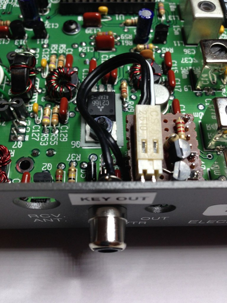
10. Make up a short cable (3″ or 4″) with the molex plug on one end. Solder the side of the cable that connects to the pin closest to the side of the board, going through hole F1, to the ground lug on the RCA connector.
11. Install the RCA connector in the hole on the bottom chassis labelled “XVTR IN”. Solder the other side of the molex plug cable to the inner conductor of the RCA connector.
12. Plus the keying circuit board into the J13 header socket on the RF board. Connect the molex plug to the molex receptor on the keying circuit board.
And that’s it. Plug one end of the RCA-RCA cable into the new RCA connector on the back on your K2, and plug the other end of the cable into the “PA KEY” RCA socket on the back of the KXPA100. Connect up a patch cord between the K2 ANT OUT and the KXPA100 RF IN, and you are good to go.
Here are some pics of the completed circuit, from above and from beneath.


